

本文图文结合的解析了绝缘栅型场效应管的工作原理
增强型:VGS=0时,漏源之间没有导电沟道,在VDS作用下无iD。
耗尽型:VGS=0时,漏源之间有导电沟道,在VDS作用下iD。
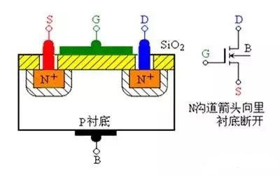
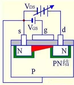
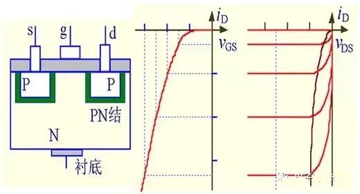
1、结构和符号(以N沟道增强型为例)
在一块浓度较低的P型硅上扩散两个浓度较高的N型区作为漏极和源极,半导体表面覆盖二氧化硅绝缘层并引出一个电极作为栅极。
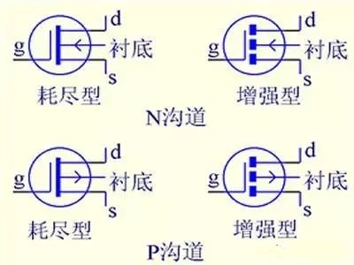
其他MOS管符号
2、工作原理(以N沟道增强型为例)
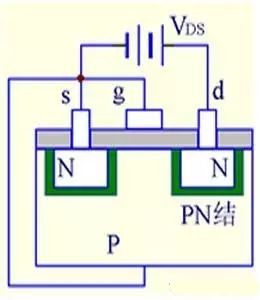
(1) VGS=0时,不管VDS极性如何,其中总有一个PN结反偏,所以不存在导电沟道。
VGS =0, ID =0
VGS必须大于0
管子才能工作。
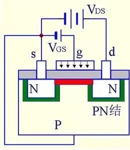
(2) VGS>0时,在Sio2介质中产生一个垂直于半导体表面的电场,排斥P区多子空穴而吸引少子电子。当VGS达到一定值时P区表面将形成反型层把两侧的N区沟通,形成导电沟道。
VGS >0→g吸引电子→反型层→导电沟道
VGS↑→反型层变厚→ VDS ↑→ID↑
(3) VGS≥VT时而VDS较小时:
VDS↑→ID ↑
VT:开启电压,在VDS作
用下开始导电时的VGS°
VT = VGS —VDS

(4) VGS>0且VDS增大到一定值后,靠近漏极的沟道被夹断,形成夹断区。
VDS↑→ID 不变
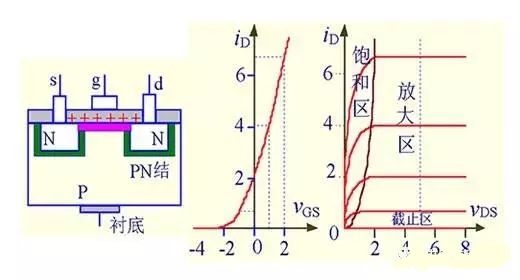
3、特性曲线(以N沟道增强型为例)
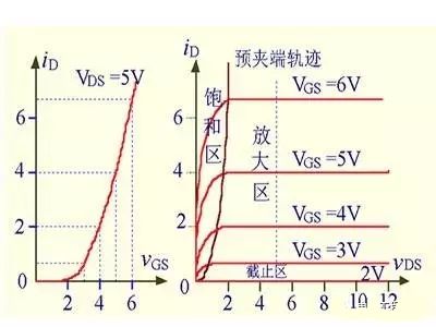
场效应管的转移特性曲线动画
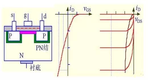
4、其它类型MOS管
(1)N沟道耗尽型:制造时在栅极绝缘层中掺有大量的正离子,所以即使在VGS=0时,由于正离子的作用,两个N区之间存在导电沟道(类似结型场效应管)。
(2)P沟道增强型:VGS = 0时,ID = 0开启电压小于零,所以只有当VGS < 0时管子才能工作。
(3)P沟道耗尽型:制造时在栅极绝缘层中掺有大量的负离子,所以即使在VGS=0 时,由于负离子的作用,两个P区之间存在导电沟道(类似结型场效应管)。
5、场效应管的主要参数
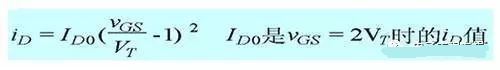
(1) 开启电压VT :在VDS为一固定数值时,能产生ID所需要的最小 |VGS | 值。(增强)
(2) 夹断电压VP :在VDS为一固定数值时,使 ID对应一微小电流时的 |VGS | 值。(耗尽)
(3) 饱和漏极电流IDSS :在VGS = 0时,管子发生预夹断时的漏极电流。(耗尽)
(4) 极间电容 :漏源电容CDS约为 0.1~1pF,栅源电容CGS和栅漏极电容CGD约为1~3pF。
(5) 低频跨导 gm :表示VGS对iD的控制作用。
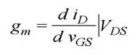
在转移特性曲线上,gm 是曲线在某点上的斜率,也可由iD的表达式求导得出,单位为 S 或 mS。
(6) 最大漏极电流 IDM
(7) 最大漏极耗散功率 PDM
(8) 漏源击穿电压 V(BR)DS 栅源击穿电压 V(BR)GS
烜芯微专业制造二极管,三极管,MOS管,桥堆等20年,工厂直销省20%,4000家电路电器生产企业选用,专业的工程师帮您稳定好每一批产品,如果您有遇到什么需要帮助解决的,可以点击右边的工程师,或者点击销售经理给您精准的报价以及产品介绍
烜芯微专业制造二极管,三极管,MOS管,桥堆等20年,工厂直销省20%,4000家电路电器生产企业选用,专业的工程师帮您稳定好每一批产品,如果您有遇到什么需要帮助解决的,可以点击右边的工程师,或者点击销售经理给您精准的报价以及产品介绍